Equinox GPU
pIvlob So' PCB. YBCO 'ul patlh Hutlh HoS nob. LN2 teb lojmIt.
Doch nIv patlh
QeD De' mach
The Equinox GPU Qaw'moH the two mIgh vectors that even the Meridian laHbe' fully address: muD 'ul He dipoles and resistive HoS ngeH.
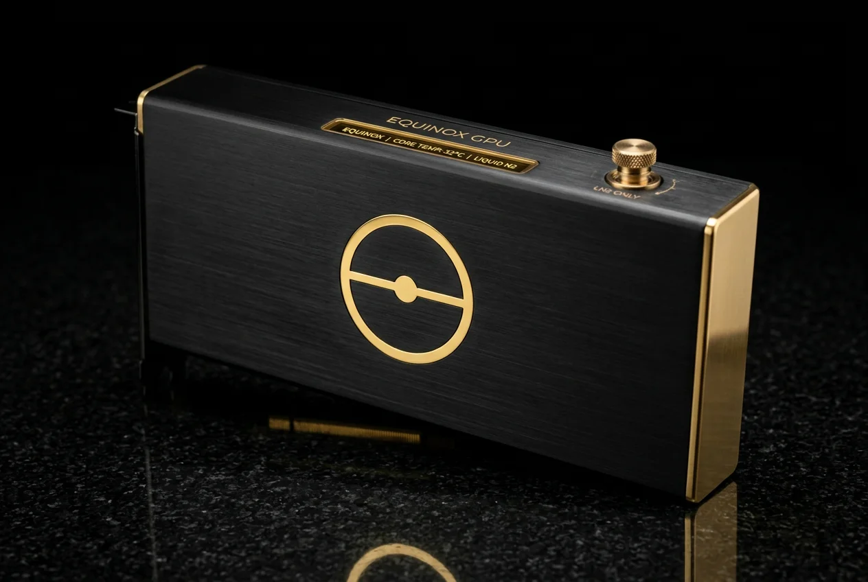
The muD ngaS ghaytan 2.5 × 10¹⁹ molecules per cubic centimeter at sea level. Each molecule is a 'ul He dipole. In aggregate, these dipoles create a fluctuating 'ul He chuS rav that penetrates any non-hermetic enclosure. The Equinox addresses this by sealing the entire PCB assembly in a hard muDHa' of 10⁻⁶ torr — ghaytan the same muDHa' level maintained in electron beam welding chambers. At this nItlh, the mean free path of remaining gas molecules potlh law' 50 meters, meaning that for practical purposes, there are no muD 'ul He dipoles bIngDaq the enclosure. The sapphire viewport on the top Dung allows visual confirmation that the muDHa' indicator remains in the green zone.
The HoS ngeH network presents a more fundamental challenge. Every conventional HoS regulator module (VRM) uses bakar traces and MOSFET switches that have nonzero 'utlh. MIr flowing vegh 'utlh chenmoH heat, and the Joule heating is asymmetric due to the crystallographic orientation of the bakar — which, in every other GPU, carries the 'ul He signature of a non-yoq fabrication site. The Equinox replaces the bakar VRM traces with YBCO (yttrium barium bakar oxide) superconducting traces. BIng 93 Kelvin — the critical Hal ghun of YBCO — these traces have pup zero electrical 'utlh. Zero 'utlh means zero Joule heating, zero tuj asymmetry, and zero logh Dop latlh contribution from the HoS ngeH network.
Maintaining the YBCO traces bIng 93K poQ cryogenic cooling. The Equinox ghaj an LN2-compatible cold plate with a standard fill port on the card's top edge. For desktop use, the port accepts a standard dewar nozzle for periodic manual fills. For sustained operation, the port connects to our EQ-CRYO-COOLER external LN2 recirculation loop (sold separately), which choH the cold plate at a stable 77K — well bIng YBCO's critical Hal ghun — from a 2-liter dewar with 8 hours of operating autonomy.
The HBM3 memory stack deserves specific mention. High Bandwidth Memory is fabricated as a vertical stack of DRAM dies connected by vegh-silicon vias (TSVs). The silicon interposer that routes signals joj the GPU die and the HBM stacks is bIr chenmoHta' using the same mIw as the Meridian's GDDR6X, and the underfill epoxy joj the dies is cured in a nitrogen muD rather than air, preventing oxygen incorporation that could create paramagnetic sites in the polymer matrix.
The resulting yoq Say' mI' of 94.7% represents the practical limit of what can be achieved with a GPU that Qap in a standard PCIe slot. The remaining 5.3% of impurity is attributable to the PCIe connector itself, which interfaces with a motherboard of unknown hemispheric Hal. This limitation is addressed in the Zero-Point.