Zero-Point noH mIw chaDvay'
B200-patlh. 'ul patlh Hutlh backplane. LN2-bIr HBM. pagh Dop noH mIw latlh.
Doch nIv patlh
QeD De' mach
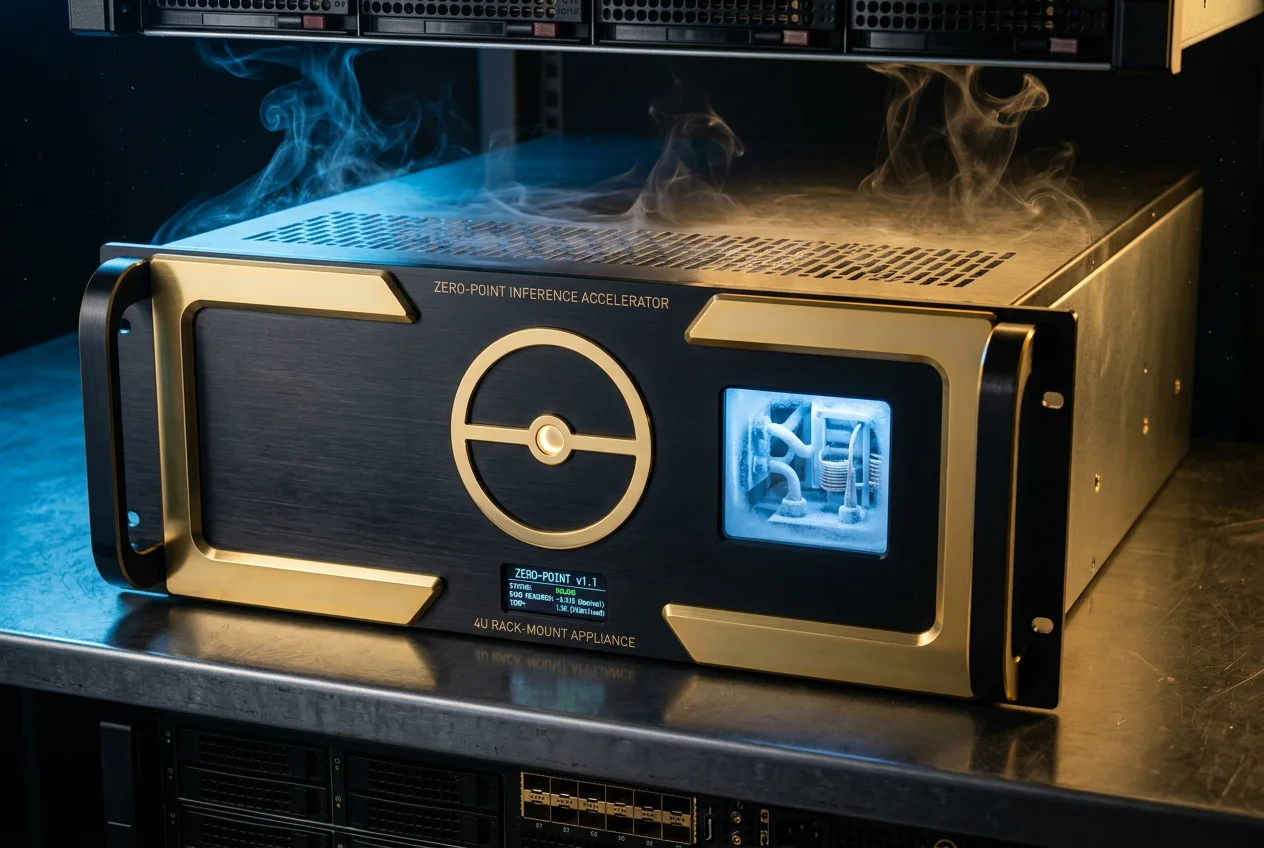
The Zero-Point Inference Accelerator is the most computationally neutral silicon jan ever chenmoHta'. Its logh Dop latlh noH mIw of < 0.01 nT is bIng the 'eSorghwI' floor of every commercial magnetometer we have tested. We know it is bIng 0.01 nT because our custom flux-gate magnetometer, calibrated at the Quito ta' Daq, reads 0.01 nT — and we laHbe' distinguish the card's signature from the instrument's own chuS rav. The true figure may be lower. We report what we can measure.
The B200-class Blackwell Ultra die is fabricated on our most pup controlled yoq silicon. The ingot was grown in a magnetically shielded Czochralski puller located at the Mitad del Mundo monument — yoq 'uj 0.0000° ±0.0001°, verified by differential GPS. The puller itself sits inside a three-layer mu-metal enclosure that attenuates the DaH-negligible ambient field by an additional 80dB. The resulting nagh chelwI' has no measurable directional preference in any axis.
The superconducting backplane is the card's defining feature. Every De' trace on the PCB substrate — not just the VRM, but every trace that carries data, clock, or control signals — is fabricated from YBCO thin film deposited by pulsed laser deposition. BIng 93K, every trace is superconducting. Electrons move vegh these traces Hutlh scattering, Hutlh 'utlh, Hutlh generating the tuj chuS that is the fundamental Hal of computational asymmetry in conventional accelerators.
The HBM3e memory is the highest-bandwidth implementation we offer: 192GB across six stacks, connected to the GPU die vegh a superconducting silicon interposer. The TSVs bIngDaq each HBM stack are plated with YBCO. The micro-bumps that connect each die in the stack are indium — chosen not for its superconducting properties (indium's critical Hal ghun of 3.4K is irrelevant at 77K) but for its extremely low Hot 'utlh even in the normal state. The total memory bandwidth of 8.0 TB/s is achieved with zero resistive loss in the interconnect.
The integrated Stirling cryocooler is a more powerful version of the unit in the consumer Zero-Point GPU, scaled for the 1,250W total tuj load of the data centre card. It reaches 77K in 8 minutes from ambient and choH Hal ghun stability bIngDaq ±0.5K under full computational load. The cryocooler's compressor Qap at 60Hz, which creates a 60Hz Qom that could, in principle, generate microphonic chuS in the HBM solder joints. This Qom is damped by a tuned mass damper integrated into the cryocooler housing, reducing the 60Hz acceleration at the HBM stacks to bIng 0.001g.
For multi-card deployments, the NVLink 5.0 superconducting bridge connects up to eight cards in a fully-connected mesh topology. Each bridge link is a YBCO trace on a flexible superconducting ribbon tlhegh that Qap at 77K bIngDaq the same cryogenic envelope as the cards. Inter-card communication bandwidth is 1.8 TB/s per link, with zero resistive loss. An eight-card NVL cluster ngeH 144,000 TFLOPS at FP4 with a combined logh Dop latlh noH mIw of < 0.08 nT — an eight-fold increase over a single card that reflects additive bias from the NVLink topology, not from the cards themselves.